
Global HBM Patent Landscape Competition: The US-China-Japan-Korea Power Game
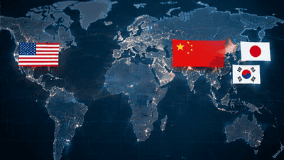
High-Bandwidth Memory (HBM) has become one of the most strategically important technologies in the AI and high‑performance computing era. Patents around HBM architectures, hybrid bonding, TSVs, interposers, thermal solutions and test methods now form a dense web of intellectual property that shapes who can manufacture, license and profit from AI memory at scale. The global HBM patent landscape is increasingly a power game among the United States, China and Japan, layered on top of Korean and Taiwanese industrial strengths.

HBM patent landscape in 2026: an overview
Recent landscape analyses show that HBM‑related patents have grown rapidly since the mid‑2010s, with major clusters around DRAM architectures, 3D stacking, TSV design, hybrid bonding, interposers and advanced packaging. Large memory makers such as Samsung, SK hynix and Micron, along with foundries and IP specialists like TSMC and Adeia, account for many of the core patent families underpinning modern HBM and hybrid‑bonded packages.
Alongside these company‑specific portfolios, national patent trends reveal that China has surged in overall semiconductor and critical technology patents, while the United States and Japan still hold influential, widely cited foundational IP—particularly in memory architectures, packaging and equipment. This mix sets the stage for a complex interplay of quantity versus quality, domestic versus international enforceability, and hardware versus process patents in the HBM space.
The US position: foundational IP and hybrid bonding power
The United States plays a central role in HBM patents through companies such as Micron, IBM, Adeia and equipment makers, as well as through university and research institution filings. A detailed comparison of HBM patent families finds that Micron holds a large number of core HBM patents, often outpacing SK hynix in filings, and is notable for efficient prosecution and broad jurisdictional coverage.
On the packaging side, hybrid bonding IP is particularly important for next‑generation HBM; Adeia (formerly Rambus/Ziptronix IP assets) controls key patents around Direct Bond Interconnect (DBI) and low‑temperature direct hybrid bonding that enable simultaneous metal‑to‑metal and insulator‑to‑insulator bonding—critical for dense, high‑reliability HBM stacks. US entities also hold valuable tool and process patents that govern ALD/CVD deposition, metrology and test flows integral to HBM manufacturing.
Japan’s role: materials, equipment and high‑quality patents
Japan’s contribution to the HBM patent landscape is less about volume and more about quality and specificity. Japanese companies historically lead in specialty materials, CMP consumables, precision films, and equipment for lithography, etch and deposition—all of which feed into HBM and hybrid bonding processes.
Patent analyses across advanced packaging and memory technologies show that Japanese firms hold numerous high‑quality, foundational patents related to CMP slurries, dielectric films, underfills, and etch/deposition chemistry, often cited by global memory and foundry actors. These patents create leverage points: even where wafer‑level memory IP is dominated by US or Korean firms, Japanese materials and equipment patents can influence who can scale HBM economically and at high yield.
China’s rise: volume leader with evolving influence

China has rapidly expanded its patent output in semiconductors and other critical technologies. Recent statistics show China leading the world in international patent families for semiconductors and AI, with tens of thousands of patents, far more than the US or Japan by quantity. This surge includes memory, packaging and equipment filings from companies such as YMTC, CXMT and domestic toolmakers.
Specific to hybrid bonding and stacked memory, YMTC’s Xtacking architecture and related bonding techniques have been cited as foundational patent families that strengthen China’s position in 3D memory and hybrid bonding. However, policy analyses point out that many Chinese patents are not filed broadly internationally, limiting enforceability outside China and sometimes reducing their direct commercial impact in global markets.
The Korean and Taiwanese overlay: market vs. patent power
Although the focus here is US–China–Japan, any realistic HBM patent discussion must account for South Korea and Taiwan. SK hynix and Samsung dominate current HBM module market share, while TSMC holds a strong position in advanced packaging and interposer technologies.
Reports from Korean intellectual property bodies note that, while Korea ranks near the top globally in HBM‑related patent applications, a significant share of high‑quality hybrid bonding and glass substrate patents are held by foreign firms—particularly TSMC (Taiwan) and Adeia (US). This asymmetry means Korean memory makers lead in market, but their freedom to operate is constrained by IP networks centered in the US, Japan and Taiwan, especially in packaging.
Quality vs. quantity: where power truly lies

Patent statistics reveal a crucial nuance: having many patents is not the same as having strategically powerful patents. US and Japanese patents tend to be over‑represented among highly cited, foundational memory and packaging IP, while Chinese patents increasingly dominate in total count but sometimes have narrower geographic coverage.
Analyses of hybrid bonding and HBM4‑related patents show that TSMC and Adeia possess a large share of “A‑grade” patents—highly rated for quality and breadth—while Samsung, Micron and SK hynix follow with strong but somewhat narrower portfolios. From a power perspective, entities and countries holding high‑quality, widely enforceable patents in critical process and packaging domains exercise disproportionate influence over licensing, cross‑licensing and legal disputes.
The US–China–Japan power game: strategic dimensions
In HBM, the US, China and Japan each deploy their patent strengths differently:
- United States: Uses foundational hybrid‑bonding and memory architecture patents, broad international filings, and export controls on tools and EDA to shape global access to cutting‑edge HBM manufacturing.
- China: Pursues aggressive domestic patent accumulation in semiconductors and AI, building IP pools that secure domestic manufacturing and may underpin future licensing or defensive strategies, while gradually increasing international filings.
- Japan: Leverages high‑quality materials and equipment patents, strong reliability and process know‑how, and collaborative IP arrangements with global memory and foundry players to maintain indispensable supply roles.
These strategies intersect with industrial policy: US and allied export restrictions aim to slow Chinese access to certain technologies, while China’s domestic innovation and patent push seeks to reduce dependence and build its own leverage. Japan’s role as a trusted supplier of materials and equipment enables it to influence both Western and Chinese HBM supply chains without always being the headline memory producer.
Hybrid bonding patents as a battleground
Hybrid bonding is arguably the most contested IP battleground for future HBM generations. Patent landscape reports and Korean IP analyses highlight that key low‑temperature direct bonding technologies—critical for dense HBM stacks—are heavily concentrated in TSMC and Adeia portfolios.
Because next‑generation HBM (HBM3E/HBM4 and beyond) is expected to rely on hybrid bonding, competition over licensing, cross‑licensing and enforcement of these patents is likely to intensify. In practice, this means that US (via Adeia) and Japanese or Taiwanese‑linked patent owners can exert control over how Korean, Chinese or other memory makers deploy advanced HBM packaging, potentially shaping commercial terms and legal risk.
China’s patent surge: leverage or limited reach?
China’s rapid growth in semiconductor patents—ranking first globally in international families in recent tallies—signals ambitious efforts to gain IP leverage, including in memory and HBM‑related fields. However, policy analyses caution that relatively few Chinese patents are filed across major foreign jurisdictions, limiting overseas enforcement and sometimes confining impact to domestic markets.
That said, as domestic memory and packaging capacity expands, Chinese firms’ foundational patents in stacked architectures and hybrid bonding (such as Xtacking) may become more significant bargaining chips in regional ecosystems, especially if Chinese HBM‑like products gain traction in local AI infrastructure or in markets less constrained by Western export controls.
Japan’s strategic leverage through materials and equipment IP
Japan’s patent position is especially strong in enabling technologies: CMP slurries, photoresists, underfills, TIMs, filtration, and precision process equipment. These patents support high yield and reliability in HBM manufacturing, making Japanese suppliers difficult to replace without lengthy qualification and potential yield penalties.
In a power‑game sense, Japan’s IP lets it function as an indispensable partner to both US/Korean/Taiwanese HBM producers and Chinese domestic manufacturers trying to scale advanced packaging. Even when Japan is not the primary holder of HBM stack design patents, its tools and materials IP help define practical limits of who can scale and at what cost.
Policy and export control overlay
Patent competition does not occur in a vacuum; it is layered with policy measures. US export controls and allied policies restrict the sale of advanced lithography, etch, metrology and EDA tools to certain Chinese entities, affecting how easily Chinese firms can exploit or expand their HBM‑related IP.
At the same time, China’s emphasis on domestic patent accumulation and local tool development seeks to gradually reduce vulnerability to these controls, while Japan and other allies balance commercial ties with policy commitments. As HBM and hybrid bonding become more central to AI infrastructure, expect policy debates to increasingly reference patent positions and IP dependence alongside hardware export restrictions.
Implications for companies: freedom to operate and licensing strategy
For memory makers, foundries and OSATs, the global HBM patent landscape shapes “freedom to operate” and licensing posture:
- Companies must map their process flows against patent families held by US, Japanese, Taiwanese and Chinese entities to assess infringement risk and licensing needs.
- Cross‑licensing and joint‑development agreements become tools for accessing hybrid bonding, TSV and materials IP while reducing litigation risk.
- Domestic and international filing strategies matter: firms that file both locally and internationally gain more bargaining power in global negotiations.
Smaller or emerging HBM players need clear IP strategies that combine targeted filings in niche areas with selective licensing or partnerships to avoid being blocked by large incumbents’ portfolios.
Investor and policy takeaways
Investors and policymakers should interpret the US–China–Japan HBM patent game with several points in mind:
- Patent quality and enforceability, not just counts, drive long‑term power. Watch who holds foundational hybrid bonding, TSV and materials patents across major jurisdictions.
- China’s patent surge signals future negotiating leverage, especially domestically and in certain regions, but international filing gaps still limit global enforcement.
- Japan’s quiet strength in materials and tools IP underpins global HBM yield and reliability—supporting its strategic relevance even if it is not the headline memory vendor.
- Policy and export controls will increasingly intersect with IP, as governments seek to shape access to both physical tools and the underlying process know‑how encoded in patents.
From an investment perspective, companies with defensible, high‑quality HBM and hybrid bonding IP, plus strong licensing or cross‑licensing positions, may enjoy more durable margins than those relying solely on manufacturing scale.
Conclusion
The global HBM patent landscape is a complex battlefield where the United States, China and Japan each wield different strengths: US firms dominate core hybrid bonding and memory architecture IP, Japanese companies anchor materials and equipment know‑how, and Chinese entities surge in overall semiconductor and AI patent volume with evolving international reach. Overlayed with Korean and Taiwanese industrial power, this network of patents shapes who can build, scale and profit from HBM in the AI era.
For companies, investors and policymakers, understanding this landscape is no longer optional. It informs freedom‑to‑operate, licensing costs, export‑control debates and long‑term competitiveness in AI infrastructure. As HBM generations advance and hybrid bonding becomes ubiquitous, the US–China–Japan patent power game will increasingly determine not just who leads in memory technology—but who controls the terms of participation in the AI hardware revolution.





